- 您现在的位置:买卖IC网 > Sheet目录1852 > MCP1824ST-3002E/DB (Microchip Technology)IC REG LDO 3V .3A SOT223-3
�� �
�
�MCP1824/MCP1824S�
�1.0�
�ELECTRICAL�
�CHARACTERISTICS�
�?� Notice:� Stresses� above� those� listed� under� “Maximum� Rat-�
�ings”� may� cause� permanent� damage� to� the� device.� This� is� a�
�stress� rating� only� and� functional� operation� of� the� device� at�
�those� or� any� other� conditions� above� those� indicated� in� the�
�Absolute� Maximum� Ratings� ?�
�Input� Voltage,� V� IN� .............................................................6.5V�
�operational� listings� of� this� specification� is� not� implied.� Expo-�
�sure� to� maximum� rating� conditions� for� extended� periods� may�
�affect� device� reliability.�
�Maximum� Voltage� on� Any� Pin� ...� (GND� –� 0.3V)� to� (V� IN� +� 0.3)V�
��Output� Short� Circuit� Duration� ................................� Continuous�
�Storage� temperature� .....................................-65°C� to� +150°C�
�Maximum� Junction� Temperature,� T� J� ...........................� +150°C�
�Operating� Junction� Temperature,� T� J� .............-40°C� to� +125°C�
�EESD� protection� on� all� pins� ...........� ≥� 4� kV� HBM;� ≥� 300V� MM�
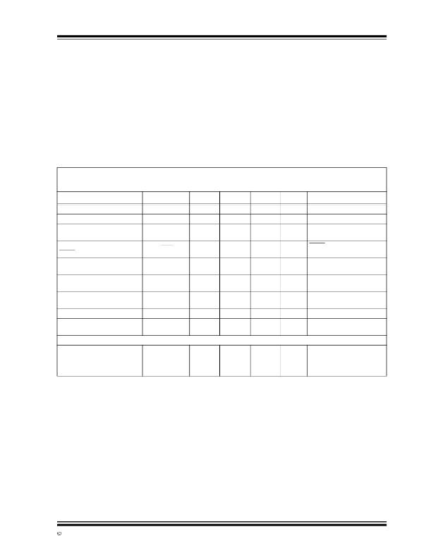
�AC/DC� CHARACTERISTICS�
�Electrical� Specifications:� Unless� otherwise� noted,� V� IN� =� V� OUT(MAX)� +� V� DROPOUT(MAX)� ,� Note� 1� ,� V� R� =� 1.8V� for� Adjustable� Output,�
�I� OUT� =� 1� mA,� C� IN� =� C� OUT� =� 4.7� μF� (X7R� Ceramic),� T� A� =� +25°C.�
�Boldface� type� applies� for� junction� temperatures,� T� J� (� Note� 7� )� of� -40°C� to� +125°C�
�Parameters�
�Input� Operating� Voltage�
�Output� Voltage� Range�
�Input� Quiescent� Current�
�Sym�
�V� IN�
�V� OUT�
�I� q�
�Min�
�2.1�
�0.8�
�—�
�Typ�
�—�
�—�
�120�
�Max�
�6.0�
�5.0�
�220�
�Units�
�V�
�V�
�μA�
�Conditions�
�I� L� =� 0� mA,� V� OUT� =� 0.8V� to�
�5.0V�
�Input� Quiescent� Current� for�
�I� SHDN�
�—�
�0.1�
�3�
�μA�
�SHDN� =� GND�
�SHDN� Mode�
�Maximum� Continuous� Output�
�I� OUT�
�300�
�—�
�—�
�mA�
�V� IN� =� 2.1V� to� 6.0V�
�Current�
�V� R� =� 0.8V� to� 5.0V�
�Line� Regulation�
�Load� Regulation�
�Δ� V� OUT� /�
�(V� OUT� x� Δ� V� IN� )�
�Δ� V� OUT� /V� OUT�
�—�
�-1.0�
�±0.05�
�±0.5�
�±0.� 17�
�1.0�
�%/V�
�%�
��I� OUT� =� 1� mA� to� 300� mA,�
��Output� Short� Circuit� Current�
�Dropout� Voltage�
�I� OUT_SC�
�V� DROPOUT�
�—�
�—�
�720�
�200�
�—�
�320�
�mA�
�mV�
�R� LOAD� <� 0.1� Ω� ,� Peak� Current�
��V� IN(MIN)� =� 2.1V�
�Pulsed� Applications�
�Maximum� Pulsed� Output�
�I� PULSE�
�—�
�500�
�—�
�mA�
�V� IN� =� 2.1V� to� 6.0V�
�Current�
�Note� 1:�
�2:�
�3:�
�4:�
�5:�
�6:�
�7:�
�V� R� =� 0.8V� to� 5.0V,�
�Duty� Cycle� ≤� 60%,�
�Period� <� 10� ms�
�The� minimum� V� IN� must� meet� two� conditions:� V� IN� ≥� 2.1V� and� V� IN� ≥� V� OUT(MAX)� +� V� DROPOUT(MAX).�
�V� R� is� the� nominal� regulator� output� voltage� for� the� fixed� cases.� V� R� =� 1.2V,� 1.8V,� etc.� V� R� is� the� desired� set� point� output�
��TCV� OUT� =� (V� OUT-HIGH� –� V� OUT-LOW� )� *10� 6� /� (V� R� *� Δ� Temperature).� V� OUT-HIGH� is� the� highest� voltage� measured� over� the�
�temperature� range.� V� OUT-LOW� is� the� lowest� voltage� measured� over� the� temperature� range.�
�Load� regulation� is� measured� at� a� constant� junction� temperature� using� low� duty-cycle� pulse� testing.� Load� regulation� is�
�tested� over� a� load� range� from� 1� mA� to� the� maximum� specified� output� current.�
�Dropout� voltage� is� defined� as� the� input-to-output� voltage� differential� at� which� the� output� voltage� drops� 2%� below� its�
�nominal� value� that� was� measured� with� an� input� voltage� of� V� IN� =� V� OUT(MAX)� +� V� DROPOUT(MAX)� .�
�The� maximum� allowable� power� dissipation� is� a� function� of� ambient� temperature,� the� maximum� allowable� junction�
�temperature� and� the� thermal� resistance� from� junction� to� air.� (i.e.,� T� A� ,� T� J� ,� θ� JA� ).� Exceeding� the� maximum� allowable� power�
�dissipation� will� cause� the� device� operating� junction� temperature� to� exceed� the� maximum� +150°C� rating.� Sustained�
�junction� temperatures� above� 150°C� can� impact� device� reliability.�
�The� junction� temperature� is� approximated� by� soaking� the� device� under� test� at� an� ambient� temperature� equal� to� the�
�desired� junction� temperature.� The� test� time� is� small� enough� such� that� the� rise� in� the� junction� temperature� over� the�
�ambient� temperature� is� not� significant.�
�2007� Microchip� Technology� Inc.�
�DS22070A-page� 7�
�发布紧急采购,3分钟左右您将得到回复。
相关PDF资料
MCP1825T-3302E/DC
IC REG LDO 3.3V .5A SOT223-5
MCP1826T-5002E/DC
IC REG LDO 5V 1A SOT223-5
MCP1827-3302E/ET
IC REG LDO 3.3V 1.5A DDPAK-5
MCP73113T-06SI/MF
IC LI-ION/LI-POLY CTRLR 10-DFN
MCP73830T-2AAI/MYY
IC BATT MGMT LI-ION 1A 6TDFN
MCP73855-I/MF
IC CONTROLLER LI-ION 4.5V 10DFN
MCT5201SR2M
OPTOCOUPLER PHOTO TRANS 6SMD
MCT62W
OPTOCOUPLER TRANS-OUT 2CH 8-DIP
相关代理商/技术参数
MCP1824ST-3302E/DB
功能描述:低压差稳压器 - LDO 300 mA CMOS LDO Vout 3.3V Ext Temp Range RoHS:否 制造商:Texas Instruments 最大输入电压:36 V 输出电压:1.4 V to 20.5 V 回动电压(最大值):307 mV 输出电流:1 A 负载调节:0.3 % 输出端数量: 输出类型:Fixed 最大工作温度:+ 125 C 安装风格:SMD/SMT 封装 / 箱体:VQFN-20
MCP1824ST-5002E/DB
功能描述:低压差稳压器 - LDO 300 mA CMOS LDO Vout 5.0V Ext Temp Range RoHS:否 制造商:Texas Instruments 最大输入电压:36 V 输出电压:1.4 V to 20.5 V 回动电压(最大值):307 mV 输出电流:1 A 负载调节:0.3 % 输出端数量: 输出类型:Fixed 最大工作温度:+ 125 C 安装风格:SMD/SMT 封装 / 箱体:VQFN-20
MCP1824ST-ADJE/DB
功能描述:低压差稳压器 - LDO 300 mA CMOS LDO Adj Vout Ext Temp Range RoHS:否 制造商:Texas Instruments 最大输入电压:36 V 输出电压:1.4 V to 20.5 V 回动电压(最大值):307 mV 输出电流:1 A 负载调节:0.3 % 输出端数量: 输出类型:Fixed 最大工作温度:+ 125 C 安装风格:SMD/SMT 封装 / 箱体:VQFN-20
MCP1824T-0802E/DC
功能描述:低压差稳压器 - LDO 300 mA CMOS LDO Vout 0.8V ETR RoHS:否 制造商:Texas Instruments 最大输入电压:36 V 输出电压:1.4 V to 20.5 V 回动电压(最大值):307 mV 输出电流:1 A 负载调节:0.3 % 输出端数量: 输出类型:Fixed 最大工作温度:+ 125 C 安装风格:SMD/SMT 封装 / 箱体:VQFN-20
MCP1824T-0802E/OT
功能描述:低压差稳压器 - LDO 300 mA CMOS LDO Vout 0.8V ETR RoHS:否 制造商:Texas Instruments 最大输入电压:36 V 输出电压:1.4 V to 20.5 V 回动电压(最大值):307 mV 输出电流:1 A 负载调节:0.3 % 输出端数量: 输出类型:Fixed 最大工作温度:+ 125 C 安装风格:SMD/SMT 封装 / 箱体:VQFN-20
MCP1824T-0802E/OT
制造商:Microchip Technology Inc 功能描述:; Input Voltage Primary Max:6V; Output V
MCP1824T-1202E/DC
功能描述:低压差稳压器 - LDO 300 mA CMOS LDO Vout 1.2V ETR RoHS:否 制造商:Texas Instruments 最大输入电压:36 V 输出电压:1.4 V to 20.5 V 回动电压(最大值):307 mV 输出电流:1 A 负载调节:0.3 % 输出端数量: 输出类型:Fixed 最大工作温度:+ 125 C 安装风格:SMD/SMT 封装 / 箱体:VQFN-20
MCP1824T-1202E/DC
制造商:Microchip Technology Inc 功能描述:; Input Voltage Primary Max:6V; Output V